Services Include
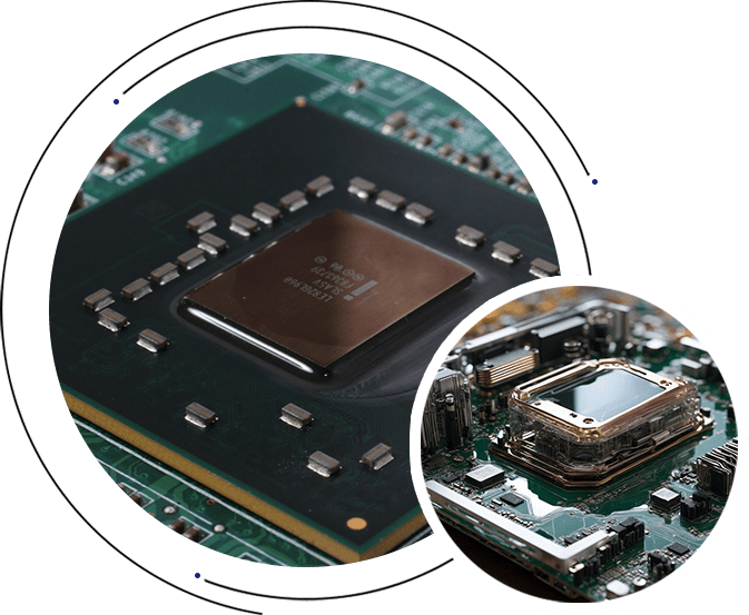
Through many years of experience and a lot of research and development with microchips, we have acquired the skills and knowledge to manipulate an IC in just about any way possible.
Our services include but are not limited to:
- Intellectual Property EoU
- World-Class Microchip Delayering
- Cross Sectioning
- Backside Poly
- Bevel
- EDX Materials Analysis
- Product Teardown
- Die Photo
- PCB Delayering
- Decapsulation
- X-Rays
- PCB & IC Analysis
- Device Manipulation
- Sample Imaging (Optical or SEM)
- Substrate
- Substrate Staining n/p
- TEM
- Scanning Capacitance Microscopy
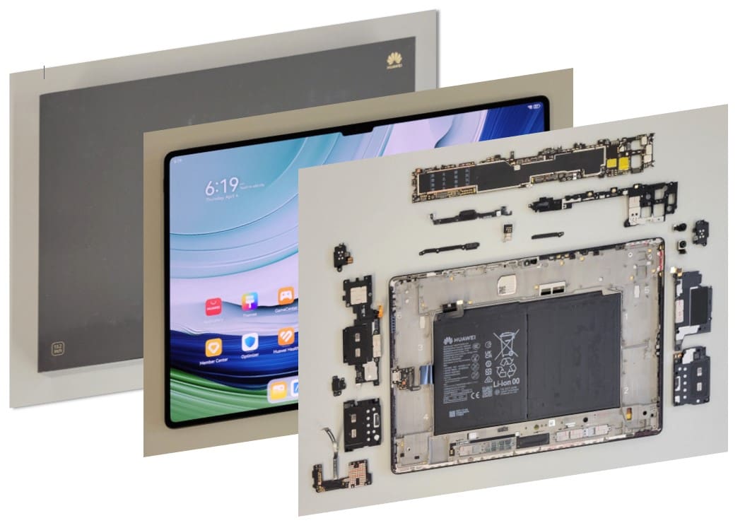
Teardown
Our product teardowns are imaged in a way that tells a story.
A product teardown can be as simple as just a teardown or as complex as tracing a chip into its product. Our IP teardowns will tell a story matching a chip to its product.
Decapsulation/Die Photo
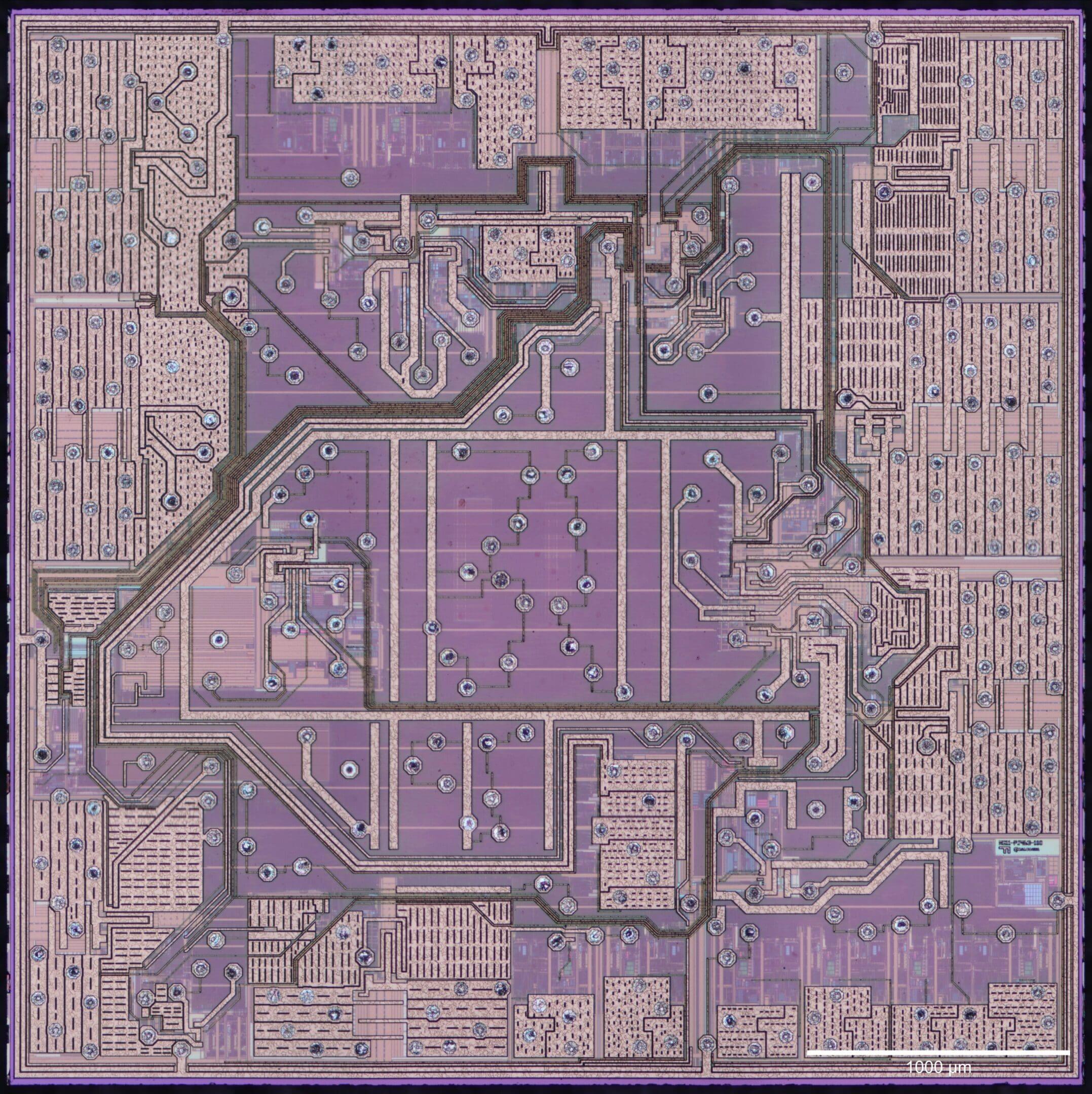
Our decapsulation process has endured much R & D and results in a non-damaged, pristine die. Our die photos are world class and will allow viewing of the top of the chip.
Cross Section
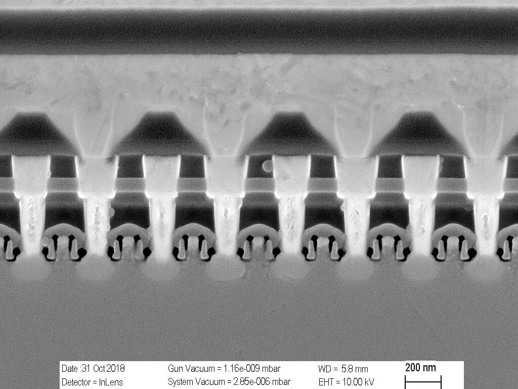
Our cross sections are done manually and not with a FIB resulting in a much longer “whole chip” cross section. This allows our clients to see all the features of the device and not just a small area. This process is used on (but not limited to) PCBs, passive, packaged IC’s, and bare die.
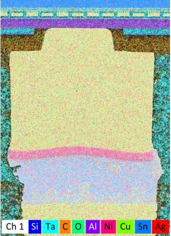
EDX Energy Dispersive X-Ray
This method is done in the scanning electron microscope and produces spectra showing the materials (elements) within the area analyzed. We can acquire spot scans, line scans, and mapping. Often used on cross-sections to show the elements that exist within the different structures (i.e. copper/aluminum circuitry, dielectrics/substrate, etc.)
Delayering
Delayering microchips is extremely difficult. It takes millions of dollars and years of R&D. We are experts at CMP and plasma technology. Here at RevEng we are proud to say that we are the best in the world at delayering microchips and can analyze down to 3 nm. We delayer chips and their packaging as well as PCB’s.
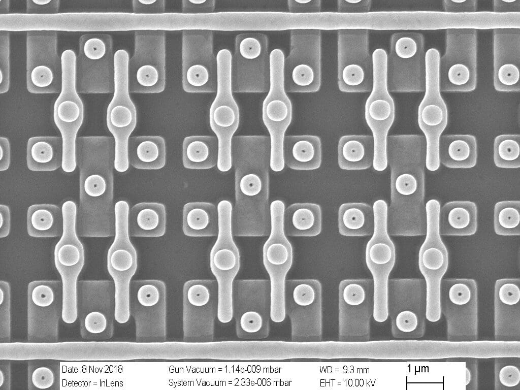

Bevel
This process allows one to view a sample of all layers (top metal to gate level) of the chip topographically. Very useful for seeing new innovations and technologies in a competing device. Also good for targeting certain layers within a structure on a chip (i.e. One can view a M3 to the gate level on SRAM or digital logic etc...)
X-Ray
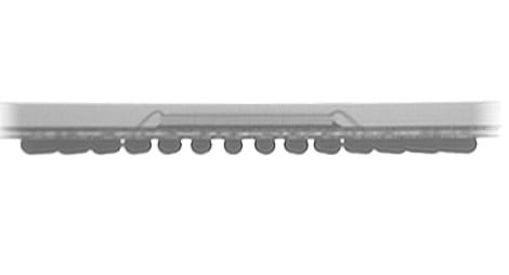
Allow us to show you what’s inside. X-Ray is an excellent, non-destructive way of analyzing just about anything prior to further analysis. Good for viewing wire and bond balls, circuitry within packaging on PCB, orientation of die, leads, etc.
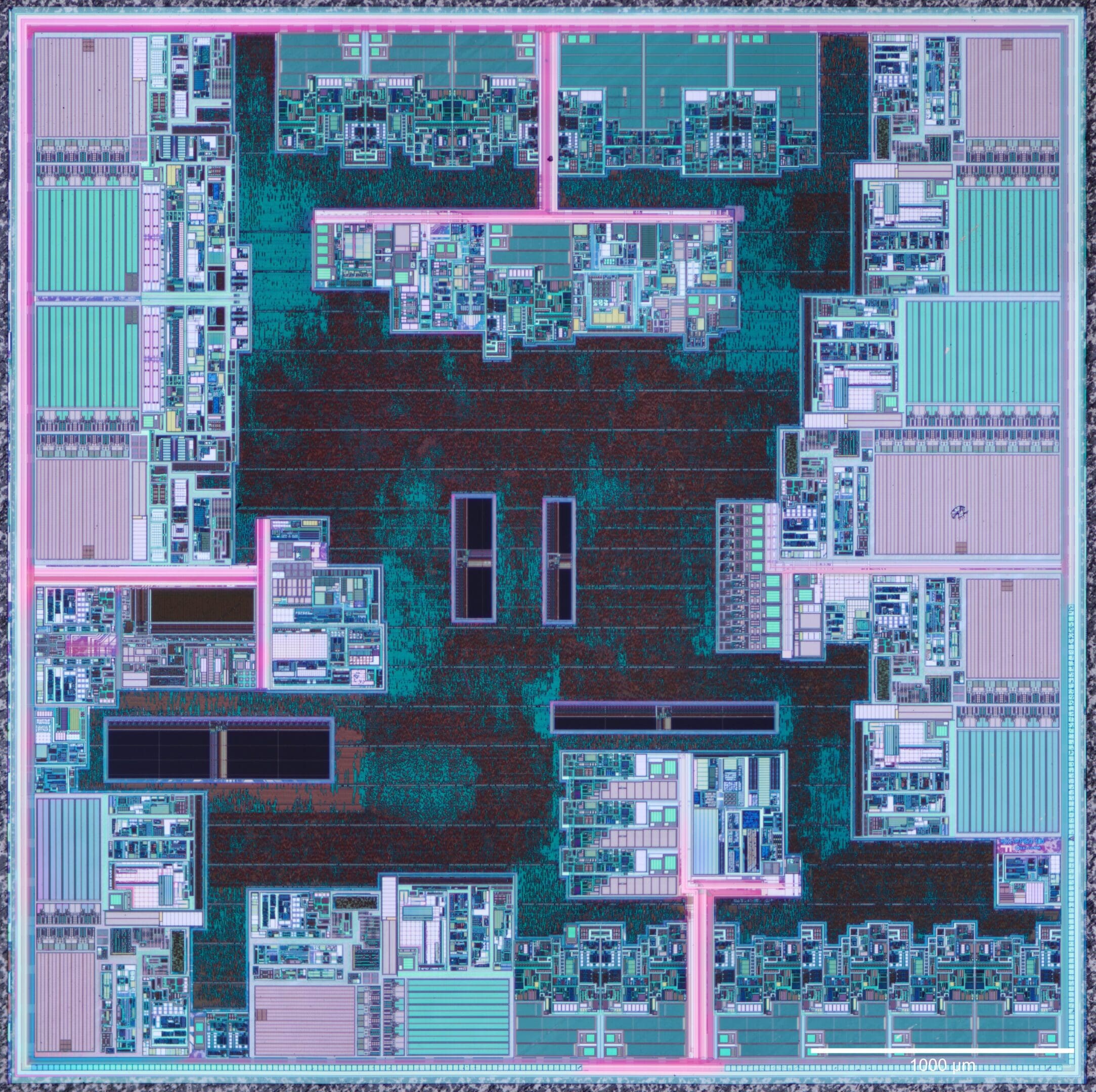
Backside Poly
This sample is prepared from the backside. All of the Si is removed in order to create an optical image showing all areas of the die. These areas include memory, digital, analog and many more. Further analysis can be done to create a "floorplan" describing the possible functions of these sections. The sample can also be viewed using a SEM to show gates and many other properties.
Substrate
A substrate sample is stripped of all circuitry and dielectrics in order to show active and inactive areas. Sometimes called a diffusion sample.
